Chip Scientist Says Nvidia’s Scaling Strategy Nears Physical Limits
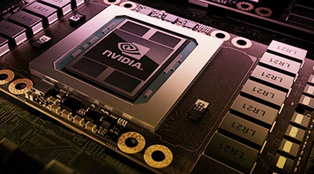
Huawei Technologies Co.’s leading semiconductor scientist cautioned about the impending physical constraints that Western chipmaking giants, such as Nvidia Corp., encounter in their quest for increasingly powerful processors, during an uncommon public appearance broadcast in China. During a marathon four-hour interview aired in late July, Liao Heng articulated his perspectives on the optimal trajectory for chip design, discussed the challenges Huawei encountered following US sanctions that severed its access to global chipmaking suppliers five years ago, and praised his company’s innovative strategy known as the Tau Scaling Law. Liao’s appearance alongside a local influencer represents a renewed expression of confidence from the Shenzhen-based semiconductor engineering leader of the nation. This follows a May keynote address entitled “New Semiconductor Path in Practice,” during which the company elaborated on its design philosophy. He argued that the long-standing trend of consistently miniaturising and increasing the density of integrated circuits is approaching its limits. Nvidia, the preeminent chip company globally, is developing increasingly larger chips that incorporate billions of transistors along with escalating quantities of high-bandwidth memory. “There has to be a limit in how they scale up with ever-increasing compute die and more HBM,” Liao stated. “The industry continues to advance, yet upon reaching that physical threshold, a significant surge is anticipated.”
Liao’s comments indicate that he aligns with a prevalent perspective that chip foundries such as Taiwan Semiconductor Manufacturing Co. and Intel Corp. may ultimately encounter limitations in their efforts to continuously shrink the size of each transistor within a chip. Both companies, along with Samsung Electronics Co., possess comprehensive roadmaps that extend several years into the future, supported by the essential advanced lithography machinery provided by ASML Holding NV. However, Huawei, restricted from accessing those systems due to sanctions imposed on China and the company, has had to adopt a more innovative approach to seek an alternative route for advancement. The company’s Tau Scaling Law suggests an emphasis on enhancing transmission speeds among components within a computer system, as the intrinsic benefits of miniaturising chips begin to wane. Huawei is poised to introduce its inaugural smartphone chip developed under this framework, utilising a technology known as LogicFolding. Liao indicated that by the end of this year, there will be a definitive comprehension of how Huawei’s alternative strategy will assist in closing the competitive gap with its rivals, particularly when its new smartphone chip is analysed by industry research entities like SemiAnalysis and TechInsights.
The increasing divergence between the US and China in their approaches to semiconductor advancements, as noted by Liao, occurs amidst escalating geopolitical tensions that are fragmenting the global supply chain into two more distinct ecosystems. “To survive, each side has to build its own complete manufacturing and supply capabilities, even without serious clashes between the two sides,” Liao stated. The rare public dialogue with a scientist central to China’s semiconductor self-sufficiency initiative illustrates the nation’s increasing determination to detach itself from Western technology in the age of artificial intelligence. During the podcast interview, the Huawei scientist presented a metaphor for the entire AI value chain, depicting it as an 18-level pagoda, thereby surpassing the layer cake framework analogy put forth by Nvidia Chief Executive Officer Jensen Huang. Liao emphasised the necessity for Chinese players at every level to provide mutual support and collaborate in order to navigate external sanctions, particularly between chip manufacturers and AI model developers.
He then showered praise on Liang Wenfeng, the founder of Hangzhou-based AI lab DeepSeek, whose cutting-edge model in 2025 triggered a multibillion-dollar selloff in AI stocks by demonstrating how Chinese developers could train systems using significantly fewer computing resources than their American counterparts. DeepSeek’s breakthrough emerged as Liang and his team pursued innovation in the model’s architectural design, considering the constraints of their limited computing resources, Liao noted. The momentum has accelerated this year, with several additional Chinese companies introducing models that surpass benchmarks. He compared Chinese AI innovation to the manner in which individuals optimise space in a confined flat, while competitors and adversaries reside in more expansive villas. Huawei is developing its AI chips to enhance efficiency-focused model architectures through what Liao referred to as a co-design mechanism. “We must increase our focus on design to exchange greater complexity for reduced consumption of computational resources,” Liao stated.